
NanoFrazor® lithography ? based on thermal Scanning Probe Lithography developed at IBM Research ? is the fastest and most versatile of all Scanning Probe Lithography techniques.
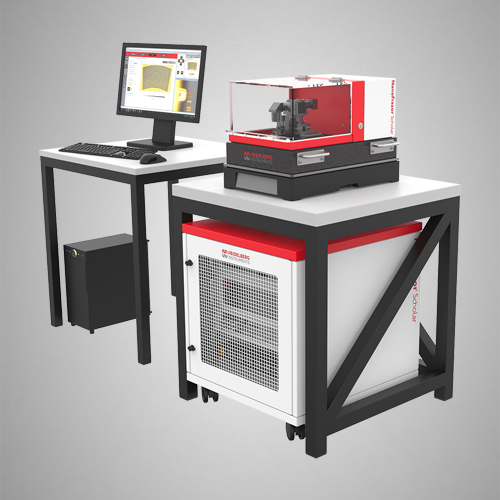
The NanoFrazor® Scholar is the entry level NanoFrazor® system and is particularly suited for academic research groups looking for an easy way to create high-resolution nanopatterns or devices. The NanoFrazor® Scholar is a compact system designed to fit in the smallest lab spaces. It can also be installed in a dedicated glovebox to enable nanolithography of sensitive materials in inert conditions.
Like all NanoFrazor® tools, the Scholar can pattern features with ultra-high resolution with no need for proximity effect corrections. All the unique NanoFrazor® capabilities like in-situ AFM imaging, accurate 3D grayscale lithography, markerless overlay or thermal material conversion are available with the Scholar.
Key Features :
- Resolution below 20 nm
- In-situ high-speed AFM topography imaging
- Samples size up to 50 x 50 mm2
- Closed-Loop Lithography
- Precise markerless overlay and stitching using in-situ AFM
- No damage of sensitive materials (no electron or ion beams)
- Alternative patterning mode: direct nanoscale thermal conversion
- Small footprint
- Easy to use (no wet development, no vacuum, etc.)
- Unique capabilities help publish in high-impact journals and receive funding for new projects.